M6 High Speed PCB: Panasonic R-5775 Low Loss Multilayer Circuit Board
(Printed Circuit Boards are custom-made products; the images and parameters shown are for reference only)
Product Overview
Introducing the M6 High Speed PCB, constructed from Panasonic Megtron6 (M6) R-5775G high speed low loss material. This advanced 4-layer circuit board features:
Copper Weight: 1oz on the outer layers.
Solder Mask: Black solder mask applied on both the top and bottom sides.
Surface Finish: Pads are plated with electroless nickel and immersion gold (ENIG).
Packaging: Every batch of 50 boards is vacuum packed for secure shipment.
.jpg)
PCB Specifications
| PCB SIZE | 95 x 96mm=1up |
| BOARD TYPE | Multilayer PCB |
| Number of Layers | 4 layers |
| Surface Mount Components | YES |
| Through Hole Components | YES |
| LAYER STACKUP | copper ------- 17um(0.5 oz)+plate TOP layer |
| Prepreg | |
| copper ------- 18um(0.5 oz) | |
| R-5775G 0.25mm | |
| copper ------- 18um(0.5 oz) | |
| Prepreg | |
| copper ------- 17um(0.5 oz)+plate BOT layer | |
| TECHNOLOGY | |
| Minimum Trace and Space: | 4 mil / 4 mil |
| Minimum / Maximum Holes: | 0.3 mm / 6.0 mm |
| Number of Different Holes: | 2 |
| Number of Drill Holes: | 6 |
| Number of Milled Slots: | 1 |
| Number of Internal Cutouts: | no |
| Impedance Control: | no |
| Number of Gold finger: | 0 |
| BOARD MATERIAL | |
| Glass Epoxy: | R-5775G |
| Final foil external: | 1.0 oz |
| Final foil internal: | 0.5 oz |
| Final height of PCB: | 0.8 mm ±0.1 |
| PLATING AND COATING | |
| Surface Finish | Immersion gold, 22% |
| Solder Mask Apply To: | Top Layer and Bottom layer |
| Solder Mask Color: | Black |
| Solder Mask Type: | Kuangshun |
| CONTOUR/CUTTING | Routing |
| MARKING | |
| Side of Component Legend | Top Layer |
| Colour of Component Legend | White |
| Manufacturer Name or Logo: | N/A |
| VIA | Plated through hole(PTH), minimum size 0.3mm. |
| FLAMIBILITY RATING | 94V-0 |
| DIMENSION TOLERANCE | |
| Outline dimension: | 0.0059" |
| Board plating: | 0.0029" |
| Drill tolerance: | 0.002" |
| TEST | 100% Electrical Test prior shipment |
| TYPE OF ARTWORK TO BE SUPPLIED | email file, Gerber RS-274-X, PCBDOC etc |
| SERVICE AREA | Worldwide, Globally. |
.jpg)
Manufacturing Process for Multi-layer PTH PCB (Via Filled)
The manufacturing process involves the following steps:
Material Shearing
Inner Layer Dry Film Application
Inner Layer Etching
Automated Optical Inspection (AOI) 1
Black Oxidation
Milling Outline Frame
Inner Layer Drilling
PTH (Plated Through Hole) 1
Inner Layer Dry Film Application
Pattern Plating
Via Filling
Outer Layer Drilling
PTH 2
Pattern Plating 2
Outer Layer Dry Film Application
Copper-Tin Electro-Plating
Peeling and Etching
AOI 2
Solder Mask Application
Silkscreen Printing
Surface Finishing
Electrical Testing
Profile Contouring
Final Quality Control (FQC)
Packaging
Delivery
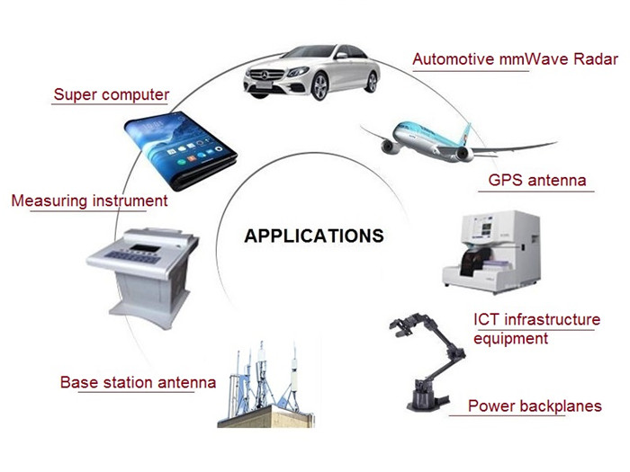
Main Applications
The M6 PCB is suitable for a variety of applications, including:
Antennas (for automotive millimeter-wave radar and base stations)
ICT infrastructure equipment
Measuring instruments
Supercomputers
.jpg)
Main Applications
The M6 PCB is ideal for a variety of applications, including:
Antennas (for automotive millimeter-wave radar and base stations)
ICT infrastructure equipment
Measuring instruments
Supercomputers
Capability and Service Area
We produce between 2500 to 3000 types of PCBs each month, serving regions including North America, Oceania, Southeast Asia, Eastern Europe, Africa, Latin America, Western & Southern Europe, Northern Europe, Central & South Asia, and the Middle East.
Explore our M6 High Speed PCB today for high-performance solutions in your electronic applications!
